Single Transistor Blocking Oscillator
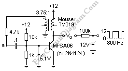
Circuit below is circuit of a transistor blocking oscillator. The transformer is phased. This cause any increase in collector current pulls the base up, further increasing the current. The transformer may the the most appropriate but not the most optimum. Any fluctuation in the collector current is fed back and reinforced because the 10k resistor biases the transistor.
The base is driven strongly negative and the transistor is cut off. The periods of cutoff and conduction then succeed automatically. At the output show us a pulse shaping circuit. The maximum value of the wave is limited by the series of resistor and Zener to 12 V (inductive effects make it considerably larger at the output, up to 20V and starting with ringing). To understand how the base and collector voltages vary, we can study the circuit using oscilloscope.
Two components are use to protect the circuit. Zener diode across the emitter junction is the more necessary. The base would be driven to -8 V in this circuit without it, which soon destroys the emitter junction. This is one of the few disadvantages of the transistor. To ensure that the rejected carries of one type predominate, the emitter must be heavily so that a high beta can be achieved. Unfortunately, this reduce the reverse breakdown voltage of the junction to only about 5 V at the same time. The action of the circuit doesn’t improved by the zener, it makes the duty cycle depart from 50% and has other deleterious effects. But that’s not a big deal. [Circuit’s schematic diagram source: Elizabeth R. Tuttle]