Complementary Pair Vertical Deflection Pre-Amp
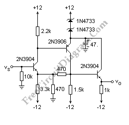
This is Complementary Pair Vertical Deflection Pre-Amplifier circuit. This circuit is modification circuit of Vertical Deflection Pre-Amplifier for 100MHz scope. This circuit remove few resistor-capacitor combination from the original circuit. That components can be removed because they tweaked the response of the amplifier at high frequencies, so no problem. The second two transistors receive +2V from the two 1N4733 5.1V zener diodes. But the two 1N4733 5.1V zener diodes can be replaced with 10V zener. Here is the schematic diagram of the circuit:
This circuit use a complementary pair of an npn and a pnp transistor. In other words coupling capacitors are not needed. This circuit has low otput impedance about 2.6R. This circuit has small AC agin of 2.0, because of strong series-shunt feedback between the two transistors.The most of the bias current of the npn transistor, flows not through the emitter capacitor but through the feedback to ground. The basic amplifier is loaded by the feedback network. [Circuit’s schematic diagram source: Elizabeth R. Tuttle]