Single Transistor Blocking Monostable

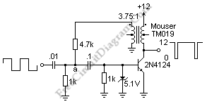
Below is a schematic diagram of blocking monostable circuit. The normal state of the transistor is off because the 10 k resistor has been removed. The conduction will be started using a positive pulse at node “a” and the transformer will do the rest. The transistor will again be turned off (by a hefty negative pulse to the base) after the brief excursion of conduction, in which the output falls to near ground.

The trigger pulses are provided by an RC differentiating circuit in this circuit, which produces narrow pulses, alternately positive and negative. The positive pulses which need only be about 1V high is the only monostable responds. The circuit will produce one low-going pulse of brief duration. The pulses will be a normal string of positive pulses if the circuit is followed by a phase inverter. There is no effort has been made to make the pulses as short as possible. These will be 100-200 us wide. [Circuit’s schematic diagram source: Elizabeth R. Tuttle]