Feedback Amplifier Using Transistors

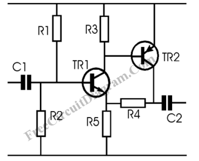
In designing small signal amplifier circuits, to achieve a specified amplifier gain we usually use opamp amplifier design to ease the setting of the gain. When the gain accuracy is not critical, we can use transistor feedback amplifier as the base of our amplifier design. Here is the schematic diagram of the transistor amplifier:

Transistor Operation
Without TR2, taking the emitter of TR1 as the output then we can see an emitter follower circuit, the voltage variation if TR1 base cause the emitter voltage to follow the base voltage. The mechanism of the emitter follower is based on the fact that the small base-emitter current will cause a large collector- emitter current, but this current cause the emitter voltage (the voltage across the emitter resistor) to rise, and the this reaction will make the base-emitter current to decrease since the current is the result of base-emitter voltage difference. This action and reaction is the basic of the feedback mechanism in the circuit. Now look at the TR2, this transistor amplify the collector current of the TR1, and now the feedback source is supplied from the TR2 collector through R4. TR2 make the collector current of TR1 very small, since the feedback is now handled by TR2. The current drawn by the base of TR1 becomes smaller, providing batter amplifier impedance at the input.
Amplifier Gain
The principle of the feedback remain unchanged, that the voltage at TR1 emitter is maintained to follow the the base voltage, and because almost all current comes from R4 (the collector-emitter current of TR1 is very small), now the voltage at the Tr2 collector (Vout) will follow the equation:
Vout=VR4+VR5;
Since VR5 follow the base voltage, and the voltage at R4 and R5 is proportional to their values, then:
VR4= (R4/R5) x VR5
The circuit is an ac amplifier, because the decoupling capacitor is used at the input and the output, so the offset error by TR1 base-emitter drop can be neglected, thus VR5=Vinput, so
Vout=VR4+Vinput;
Vout=((R4/R5)xVinput)+Vinput;
Vout=(1+(R4/R5))xVinput;
You get 1+(R4/R5) as the amplifier gain of this transistor circuit.
The Amplifier Impedance
For simplification, since the current drawn by TR1 base is very small, we can assume that the amplifier gain of the input depends only on R1 and R2, so the input impedance is R1 and R2 combination in parallel circuit (since the supply is modeled as a short circuit in ac analysis). How about the output impedance? You can see the output is not symmetric, you can drive the output instantly to charge the load capacitance because the transistor TR2 is not limited by any resistor, but if now the output have to fall down to zero, the discharging process of the capacitor will be slower because it should flow through R4 and R5. I think you can assume the output impedance as the value of R4 and R5 combination in series circuit, this assumption is safe for you worst case condition.
DC Amplifier
For DC amplification, as long as the input voltage level is always above TR1 base-emitter bias voltage (about 0.7 volt for silicon transistor), you can use the circuit as DC amplifier by removing the capacitor C1 and C2, and the bias resistor R1 and R2. The output will be valid product of the input and the amplifier gain.
Amplifier Output Protection
You can insert a resistor between the output tap and the TR2 collector, and the output is tapped at the junction of the inserted resistor and the R4. This will prevent the excessive current at TR2 when the output is shorted to ground. Please note that this resistor insertion will limit the maximum output voltage of this amplifier circuit. Select the optimal value between protection and the desired upper voltage limitation.