Wien Bridge Oscillator: The Circuit Schematic Diagram and The Design Formula
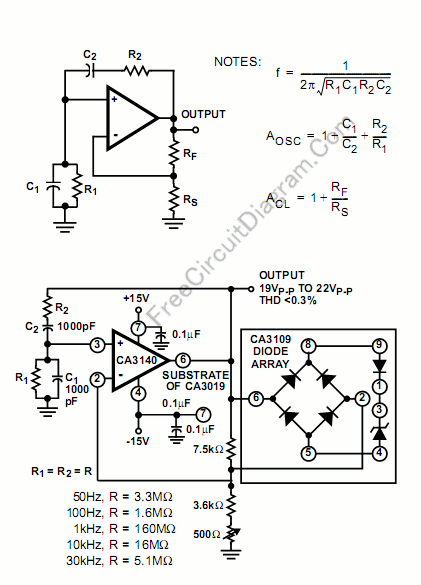
The excellent high input impedance, high slew rate, and high voltage qualities of CA3140 op-amp make it suitable for Wien-bridge sine wave oscillator. The basic circuit for Wien-bridge sine wave oscillator is shown in the figure below (the upper part). You can see the formula in the figure, when R1=R2=R, and C1=C2=C, then the formula would be a very simple and familiar f = 1/(2piRC) , and the gain required for oscillation, AOSC, is equal to 3. If C2 is multiplied by a factor of four and R2 is divided by a factor of four, the gain required for oscillation becomes 1.5, thus a potentially higher operating frequency closer to the gain bandwidth product of the CA3140 becomes possible. Here is the circuit’s schematic diagram:
The oscillation stabilization should be done, and various methods has been implemented in practice. If this the gain is not stabilized the the oscillation will either diminish or increase until distorted terribly. The feedback element RS is usually replaced with some variable resistance element. Thus, using some control methods, the value of RS is dynamically adjusted to keep constant oscillator output. A thermistor, a FET channel resistance, a lamp bulb, or other device whose resistance increases as the output amplitude is increased are a few common elements that has been implemented for this purpose.
The lower figure shows another method to stabilize the oscillator using a zener diode which shunt the feedback resistor to decrease the op-amp gain. The zener diode’s impedance will decrease as the output signal amplitude increases, resulting in more feedback with consequent reduction in gain, stabilizing the amplitude of the output signal. Using this method which employ a combination of monolithic zener diode and bridge rectifier circuit tends to provide a zero temperature coefficient for this stabilization system.
Unlike lamp bulb that has thermal time constant or RC network that is usually used in detector networks, there’s no lower frequency limit in this circuit since the bridge rectifier system has no time constant. As an example, using 1µF polycarbonate capacitors and 22M for the frequency determining network, the operating frequency would be 0.007Hz. To prevent the output signal from becoming slew-rate limited, the amplitude should be reduced as the frequency is increased. An output frequency of 180kHz will need a 9V/µs slew rate when its amplitude is 16VP-P. [Circuit’s schematic diagram source: Intersil’s CA3140 Op-Amp Application Notes]