Low-Drop-Out (LDO) Low-Voltage Linear Regulator Using NCP2860 IC
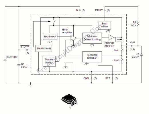
This low drop out (LDO) voltage regulator need only few components, with very low noise and very low drop-out voltage. The circuit illustrated in the schematic diagram below gives a fixed 2.77 volt output, but this output voltage can be adjusted using two additional resistors.
This circuit capable to supply 300 mA load from 3.0 V to 6.0 V input. If wished, the “SET” pin enables to adjust the output voltage level that then depends on the voltage applied to this pin. The NCP2860 has excellent performance of transient responses, PSRR and noise, make it a suitable solution for audio applications (e.g., audio amplifier drivers). Here are the key features:
- Very Low Consumption in Shutdown Mode (10 nA)
- High Power Supply Rejection Ratio (60 dB @ 1.0 kHz)
- FAULT Indicator
- High Output Current (300 mA Max)
- Low Output Voltage Noise: 60 uVrms
- Pb-Free Package is Available
- Low Dropout (150 mV @ Iout = 300 mA)
- Thermal Overload and Short Circuit Protections
- Programmable Output Voltage
- Soft-Start
As shown in the schematic diagram, the output is set to 2.77 V because the “SET” pin is grounded. To program the regulator for different output voltage, a portion of the output voltage must be applied to the “SET” pin. See the figure below:
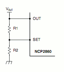
If a (R1, R2) resistors divider is used, then:
Vout = (1 + R1/R2) * VrefTherefore, as Vref typically equals 1.244 V:
Vout = 1.244 * (1 + R1/R2).
Now if R1 and R2 are high impedance resistors, the leakage current that is absorbed by the “SET” pin, may have to be taken into account as follows:
Vout = [1.244 * (1 + R1/R2)] + (R1*Ilk) where Ilk is the “SET” pin leakage current.If the output voltage is directly applied to the “SET” pin,
Vout = Vref = 1.244 V
[Circuit’s schematic diagram source: On Semiconductor Application Notes]