Notch Filter: The Circuit’s Diagram and The Design Formula
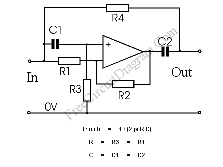
Notch filter is known as band-cut filter or band-reject filter. The fuction of this filter is to remove some frequency portion of a signal. The schematic diagram of this filter circuit, a second order notch filter is depicted in the figure below.
The formula is actually complicated, but by taking the R3=R4 and C1=C2, the filter’s frequency response formula become very simple, as shown in the figure above. By selecting C1, C2 = 47 nF, R1, R2 = 10 k, R3, R4 = 68 k, you’ll get a frequency respon of 50Hz notch, similar to hum filter in our previous circuit ( hum filter using op-amps and hum filter using transistor).
Related posts:
TDA7056 3W BTL Mono Audio Power Amplifier
Low Distortion Adjustable Audio frequency Oscillator
Audio Power Amplifier for AM Radio
LED Audio Level (VU) Indicator and Alarm: The Dot Turns to Bar When The Signal Reach The Maximum Lev...
Speaker Protector, Don't Connect Your Speaker Before The Amplifier Is Powered