Split-Phase Data Synchronization and Decoding
A split-phase data signal consists of a series of binary digits that occur at a periodic rate, as shown in waveform A in the timing chart. The weight of each bit, 0 or 1, is random, but the duration of each bit and, therefore, the periodic bit rate, essentially is constant.
A clock that is synchronized with the data bit is needed to detect and process the incoming signal. The important thing is that this clock signal should be derived from the data signal. To recover the clock and the data, a phase-lock techniques can be used. Data transition contain information about timing. This data transition can be in positive or negative direction, but both polarities have the same meaning for timing recovery. The phase of the signal determines the binary bit weight. A binary 0 or 1 is a positive or negative transition, respectively, during a bit interval in split-phase data signals.
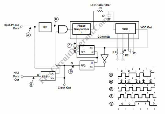
To mark the locations of the data transitions, the split-phase data input A is first differentiated . The differentiated signal B, which is twice the bit rate, is used to gate the CD4046B. Phase comparator II in the PLL is used because of its insensitivity to duty cycle on both the signal and comparator inputs. The VCO output is fed into the clock input of FF1, which divides the VCO frequency by two. The PLL tracks the differentiated signal B during the on intervals, and remembers the last frequency present and still provides a clock output during the off intervals. The VCO output is inverted and fed into the clock input of FF2, whose data input is the inverted output of FF1. FF2 provides the necessary phase shift in signal C to obtain signal D, the recovered clock signal from the split-phase data transmission. The output of FF3, E, is the recovered binary information from the phase information contained in the split-phase data. A string of alternating 0s and 1s that precede the data transmission is used to provide initial synchronization of the PLL system. [Schematic diagram source: Texas Instruments Application Report]