Frequency Doubler with 4011
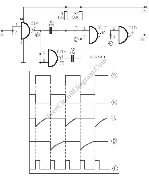
This is a circuit of Frequency Doubler using 4011. This circuit uses one CMOS quad, two input NAND gate package type 4011. This circuit consist of two differentiating networks R1/C1, R2/C2, an inverter IC1B and NAND gate IC1A, IC1D, IC1C and function as input and output buffers. Figure below shows the schematic diagram of the circuit and the pulses in different test points in the circuit:
[Source: Sam Electronic Circuit]