Pulse Delay Generator
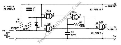
This circuit is a Delayed Pulse Generator that is used to provide pulse rate and independent control of initial delay. The pulse generator of this circuit is IC1c which the operation is depended on the normally low O/P of the IC1a. The PB1 is used to make the circuit input goes low. When PB1 is pressed, IC1b O/P goes high and the circuit O/P goes low thus replicating the input. Here is the schematic diagram of the circuit:
The point where IC1a O/P goes low is charged by capacitor C1 via R2. This action will cause pulse generator IClc to start and “rapid fire” pulses appear at the circuit O/P. C1 will discharged rapidly via R1 and D1 when the circuit input returns to the high state. The pulse rate is controlled by C2 and R3 while C1 and R2 control the initial delay. Using the shown values, the pulse rate of this circuit is 200/300Hz and delay of 0.5 seconds depending on supply voltage. PB1 can be replaced by a common emitter transistor stage or an open collector TTL gate. [Circuit’s schematic diagram source: seekic.com]