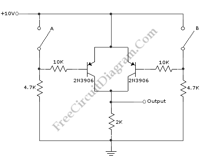
This schematic diagram shows a circuit of basic logic gate circuit. This PNP transistor circuit can act as OR gate or AND gate. If the input is closing of switch, this circuit acts as AND gate. This circuit acts as OR gate when the input is opening of switch. The phase inversion of input does not complicate overall circuitry. Here is the schematic diagram of the circuit:

Possibly Related Articles:
- Single Gate Relaxation Oscillator
Below is a relaxation oscillator circuit using a 74HC14, an inverter with a Schmitt trigger input. It’s mean that the transition point for an increasing input is higher in voltage... - Bulk Transistor Tester – An Easy Transistor Gain Classifier
This transistor tester is very helpful if you need to sort bulk transistors. In some market, if you know where to find it, sometimes you can get transistors sold in... - SCR Basic Operation
The diagram below shows us a simple block construction of an SCR (upper left) and its schematic diagram (upper right). The lower diagram shows us the operation of a PNPN... - DIAC Basic Operation
Diode for alternating current is a trigger diode which conducts current only after the DIAC reach the breakdown voltage. The breakdown voltage of DIAC is 30 V. It has construction... - SIDAC Basic Operation
Silicon Diode for Alternating Current, SIDAC, is a multilayer silicon semiconductor switch. This component is triggered by voltage and can be operated as bidirectional swtch. Usually, this SIDAC is used... - TRIAC Basic Operation
Triode for alternating current,TRIAC, is an electronic component that can control power in two direction in an AC circuit. The figure (a) shows the block construction and schematic symbol of... - Single Transistor Blocking Monostable
Below is a schematic diagram of blocking monostable circuit. The normal state of the transistor is off because the 10 k resistor has been removed. The conduction will be started... - Single Transistor Blocking Oscillator
Circuit below is circuit of a transistor blocking oscillator. The transformer is phased. This cause any increase in collector current pulls the base up, further increasing the current. The transformer... - Negative to Positive Supply Logic Level Shifter
This is a simple circuit for negative to positive supply logic level shifter. This circuit used to shift the logic level from minus to ground (such as MOS) to any... - Complement Phase Inverter with Single Transistor
This is a complement phase inverter circuit. Sometimes this circuit called a paraphase amplifier circuit. This circuit has two output signals that is have sufficient “headroom” because this circuit is... - Interfacing High Power Load to Logic Level with Optocoupler
Interfacing high power load can be done in many ways, such as using voltage divider resistors, transformer, or optocoupler. In the circuit shown below , an optocoupler method is presented.... - Crystal Oscillator Using Transistor, Capable of Overtone Operation
This circuit is a simple crystal oscillator that can be operated in overtone mode. Overtone mode permit the operation at higher frequency than specified by the crystal. The circuit uses...
| 

