52W SMPS AC-DC Adapter

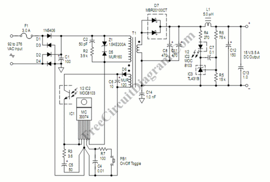
This SMPS AC-DC converter gives good efficiency. Test data shows efficiency of 83.2% at 115 Vac input and 6A output current, and 85.4% at 230 Vac input and 6A output current. Moreover, the input voltage range is universal, accommodating 92 to 276 Vac variation with only 24 mV change in the output voltage. Here is the schematic diagram of the circuit:

C8, C11 = Sanyo Os–Con #16SA1000M, 1000 µF/16V.
C12 =Sanyo Os–Con #10SA150M, 100 µF/16V.
IC1 =MC33374 mounted on Aavid #604953B02500 extruded heatsink. The heatsink must be drilled and tapped to allow device & PCB attachment.
Z1 =1.5KE200A with cathode lead soldered in the center of a 5/8” x 3/4” x 0.025” thick U–shaped copper heatsink.
D7 =MBR20100 mounted on Aavid #590302B03600 heatsink.
L1 =Coilcraft PCV–0–332–10, 3.3 µH, 0.005 ohm.
T1 =
Coilcraft W7518–A
Primary: 34 turns of # 24 AWG, Pin 9 = start, Pin 6 = finish.
Two layers 0.002” Mylar tape.
Secondary: 5 turns of # 20 AWG, 2 strands bifilar wound, Pins 4 and 5 = start, Pins 1 and 2 = finish.
Two layers 0.002” Mylar tape.
Auxiliary: 4 turns of #24 AWG wound in center of bobbin, Pin 10 = start, Pin7 = finish.
Two layers 0.002” Mylar tape.
Gap: 0.022” total for a primary inductance (LP) of 290 µH, with a primary to secondary leakage inductance of 7.2 µH.
Core: TDK PC40 EI28Z, PC40 material.
Bobbin: TDK BE–28–1110CPL, Pins 3 and 8 removed.
Toggling off PB1 power push button at Vin= 115 Vac result in 0.07 W power consumption, and 0.17W at Vin= 230 Vac. This very low power consumption in the off state is environmentally friendly. [Schematic diagram source: Motorola Analog IC Device Data]