JFET Sample and Hold Circuit
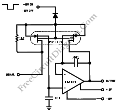
This is JFET sample and hold circuit. In this circuit, the logic voltage is applied simultaneously to the sample and hold JFETs. Here is the circuit :

The errors due to rds(on) of the JFETs can be minimized by matching feedback capacitance and resistance and input impedance. The circuit performance is greatly improved because of matched leakage currents of the FM1109 monolithic dual and the inherent matched rds(on). [Source: National Semiconductor Application Note]