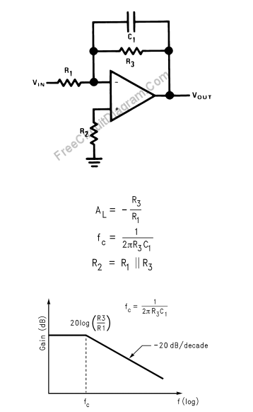
First Order Low-Pass Active Filter: The Circuit Schematic Diagram and The Design Formula

The simple low-pass filter is shown in Figure below. The filter has a 20dB/decade roll-off after its corner frequency fc. Its low-pass frequency gain (f->0) is defined by R3/R1. This allows low-frequency gains other than unity to be obtained. R2 should be chosen equal to the parallel combination of R1 and R3 to minimize error due to bias current.
LMV721/722 is recommended for the op-amp, but any high impedance and high gain op-amp is applicable. For single stage filter, 5% tolerance is adequate, but 1% resistors is recommended if the filter is used as cascaded part of third or higher odd order filter. [Circuit’s schematic diagram source: National Semiconductor’s Application Notes]