Synchronized Mains Voltage Power Control
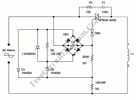
A step-down circuit used to approximately divide by two the rms voltage between the line input and the inductive load (L1) is shown on circuit diagram below. A turn-on delay of approximately 7 ms is provided by C2 and R3.
We can discharge C2 at each line zero voltage using diode bridge, with diodes D1 and D2 and R2 resistor. The voltage charge will be reset at each new half line cycle, and the turn-on delay will be maintained the same.
Through R3, the Transil reduces the power dissipation. Here’s the circuit diagram:
Note: Transil is STMicroelectronics trademark for their transient voltage suppression (TVS) diode. [Souce: STMicroelectronics Application Note]