SCR Basic Operation
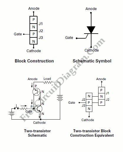
The diagram below shows us a simple block construction of an SCR (upper left) and its schematic diagram (upper right). The lower diagram shows us the operation of a PNPN device can best visualized as a specially coupled pair of transistor. When a proper gate signal is applied to the base of the NPN transistor, the connections between the two transistors trigger the occurrence of regenerative action.
The combined hFE of the specially coupled two transistor feedback amplifier is less than unity because normal leakage current is so low, thus keeping the circuit in an off-state condition. The NPN transistor is biased into conduction which in turn biased the PNP transistor into conduction by a momentary positive pulse applied to the gate. The specially coupled transistor saturate because the effective hFE momentarily becomes greater than unity. Current through the transistor is enough to keep the combined hFE greater than unity when it’s saturated once. Until it is turned off by reducing the anode-to-cathode current (It) so that the combined hFE is less than unity and regeneration ceases , the circuit is remain on. This threshold anode current is the holding current of the SCR. [Circuit’s schematic diagram source: littlefuse.com]