Programmable Photovoltaic Transimpedance Circuit

Photovoltaic transducers has been widely used in medical, consumer, scientific instrumentation, and industrial applications. Photovoltaic sensors is a solid-state devices and available for wide range of wavelength response, cover from infrared, visible, and ultraviolet spectrum. This characteristic make this type of transducer applicable in diverse jobs such as colorimetry, chemical spectral analysis, non-contact thermometry, non-invasive blood-gas monitoring, and flame detection. The basic signal conditioning circuit for photovoltaics is the current-to-voltage or transimpedance amplifier.

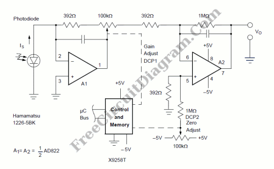
The schematic diagram shown in the figure combines two Intersil X9258T digitally controlled potentiometers with an AD822 low noise dual opamp to create a wide dynamic range, a flexible, digitally calibrated transimpedance amplifier topology that can be used with virtually any photovoltaic detector technology. The amplifier output is given by:
VO = IS(1MOhm)( 1 + P1)/(256 – P1), where P1 is the 8-bit (0 to 255) digital value written to DCP1.
One of the interesting feature of this circuit is the pseudo-logarithmic characteristic of the circuit’s transimpedance gain as a function of P1. The transimpedance gain of this amplifier varies over the range of 1/256 megohm to 256 megohm as the programming of DCP1 varies from 0 to 255 while gainfactor resolution never gets worse than 10% per P1 increment over an 400:1 (52dB or nearly 9 bit) range of 50K to 20MOhm. Transimpedance settings covering an even wider span are accessible, 4K to 256M? corresponding to fullscale IS values from 1mA to 16nA, albeit with reduced resolution. A linear gain adjustment cannot achieve both a multi-decade gain adjustment range and good adjustment resolution throughout the range.
Another feature of this circuit is the independence of gain of both DCP1 element and wiper resistances. Using the pot wiper as an input terminal effectively moves element tempco and wiper contact resistance errors inside the feedback loop of A1, thus removing them as gain-error terms and thus improving the time and temperature stability of the gain setting.
DCP2 is used to null the amplifier zero point. It varies the voltage at the noninverting input of A2 by ±2mV with a resolution of 16uV. [Source: Intersil Application Notes]