Logic Probe with Pulse Indicator

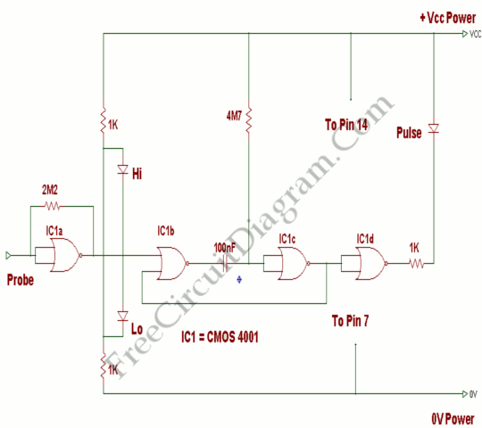
A single CMOS IC is used on this logic probe. This logic probe shows three logic condition, High, Low, and Pulsing. Ind addition, there is no LED’s will glow if the probe input is neither hi or lo ( the high impedance state of tri-output logic IC’s). Here’s the circuit diagram:

This logic probe using power from the logic circuit under test; CMOS IC enables logic circuit is used to test using voltages from 3 to 15 volts. IC1a is used as a buffer with a difference. Under no input, i.e. the gate will oscillate due to feedback from the 2M2 resistor since the probe not connected to circuit. IC1a output voltage is approximately half from supply voltage. The Hi and Lo logic indicator LED’s are connected to a potential divider. This potential divider consist of two 1K resistors. When there is no input, junction voltage is half supply voltage or high impedance no LED’s will glow. IC1a will rest in a permanent state because of Hi or Lo logic condition. This is indicated by either the Hi or Lo LED illuminating. Hi and Lo LEDs will light dimly with a fast oscillator or clock signal. This is the reason for IC1b and IC1c. These two gates form a monostable oscillator, 100nF capacitor and 4M7 resistor determine the time constant. This is effectively slowed using clock signal as the monostable is continually triggered and retriggered. IC1d works like a buffer to drive the pulsing LED. [Source: Hobby Project]